FC150
![]()
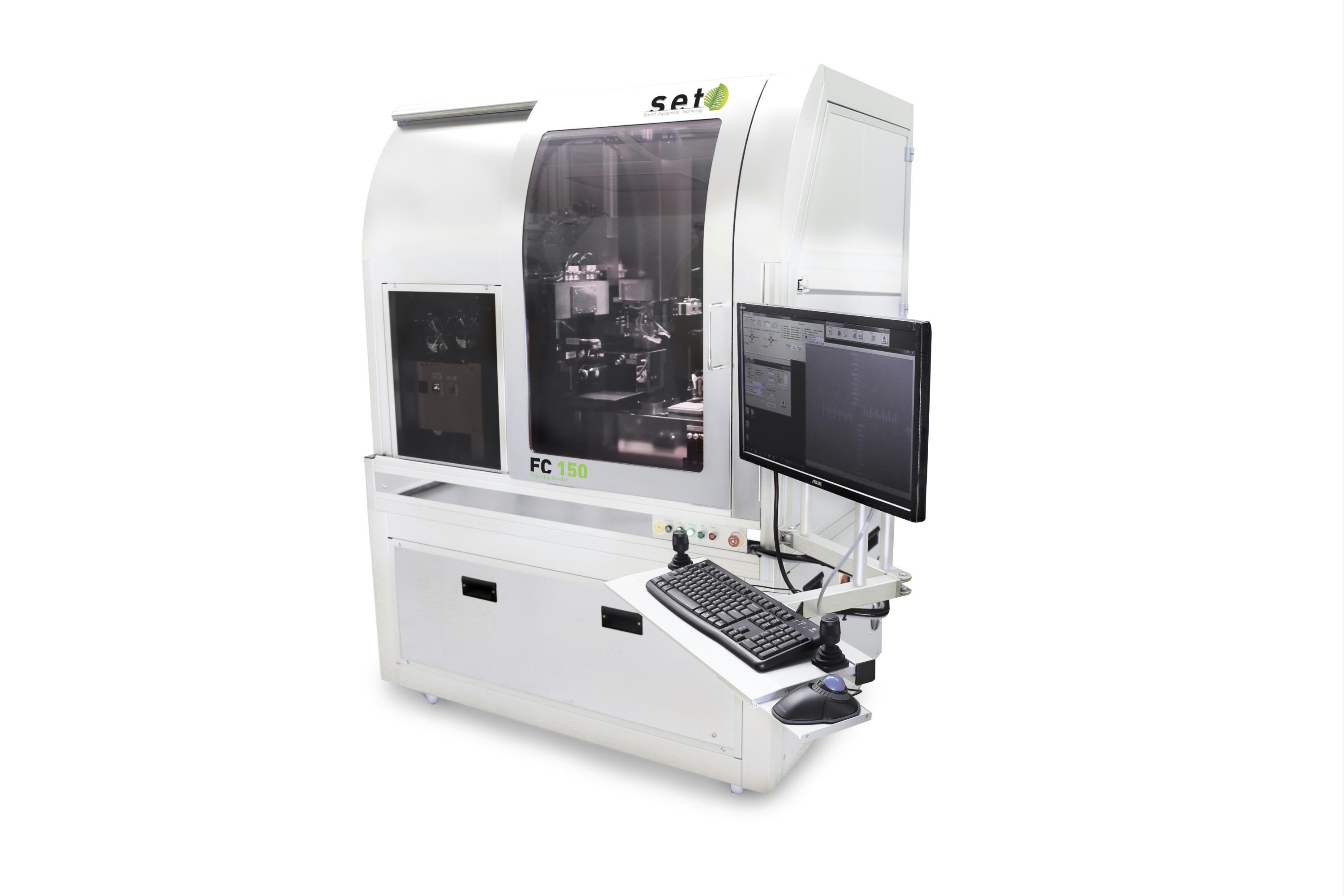
With ± 0.5 µm placement accuracy and ± 1 µm post-bond accuracy, the SET FC150 Die/Flip Chip Bonder offers the latest evolutions in bonding techniques. With configurations ranging from manual to full automation, the FC150 provides development and production capabilities on a single upgradeable cost-effective platform. The high degree of flexibility offered on the FC150 makes it the machine of choice for advanced research with the ability to move directly into pilot production.
Able to level, align and bond components ranging in size from 0.2 to 100 mm, the FC150 supports a complete range of bonding applications, including Reflow, Thermo-compression, Thermosonic, Adhesives and Fusion bonding. Active leveling is made possible through a motorized pitch & roll system combined with autocollimation or laser leveling. Designed to maximize accuracy and versatility, the FC150 answers almost every need in high-end bonding applications.
Key Benefits
![]() ± 1 µm post-bond accuracy and 20 µradian leveling guarantee high yields on the most advanced products
± 1 µm post-bond accuracy and 20 µradian leveling guarantee high yields on the most advanced products
![]() Semi-Open Confinement Chamber for Oxide Reduction (option)
Semi-Open Confinement Chamber for Oxide Reduction (option)
![]() Air bearing construction on a granite structure ensures long-term stability and reliability
Air bearing construction on a granite structure ensures long-term stability and reliability
![]() Compression, Z-control and temperature profiling, together with process monitoring, maximize process control
Compression, Z-control and temperature profiling, together with process monitoring, maximize process control
![]() Optical automatic leveling and alignment enables hands-off operation for production applications
Optical automatic leveling and alignment enables hands-off operation for production applications
![]() Nanoimprint Lithography option with Hot Embossing or UV-NIL process without compromising the bonding capability
Nanoimprint Lithography option with Hot Embossing or UV-NIL process without compromising the bonding capability
Process Capabilities
The FC150 accommodates a wide variety of materials, including extremely fragile materials such as GaAs and HgCdTe and processes: ![]() Die Bonding, Flip Chip Bonding
Die Bonding, Flip Chip Bonding![]() Mass Reflow, In-Situ Reflow, Fluxless Eutectic Bonding
Mass Reflow, In-Situ Reflow, Fluxless Eutectic Bonding![]() Thermocompression, Ultrasonic and Adhesive Bonding
Thermocompression, Ultrasonic and Adhesive Bonding![]() Gold, Gold/Tin, Indium, UV or Thermal Cure Adhesive, Polymers...
Gold, Gold/Tin, Indium, UV or Thermal Cure Adhesive, Polymers...![]() Fragile Material Compatibility: InP, GaAs, MCT...
Fragile Material Compatibility: InP, GaAs, MCT...
Bond process changes are easily achieved.
Applications
![]() Chip-to-Chip, Chip-to-Substrate Bonding, Chip Stacking
Chip-to-Chip, Chip-to-Substrate Bonding, Chip Stacking
![]() 3D Integration
3D Integration
![]() Optoelectronic & Photonic Devices Assembly
Optoelectronic & Photonic Devices Assembly
![]() MOEMS, MEMS, MCM
MOEMS, MEMS, MCM
![]() Nanoimprint Lithography: Aligned UV-NIL and Hot Embossing on Wafer
Nanoimprint Lithography: Aligned UV-NIL and Hot Embossing on Wafer