FPA & IR, UV, X-Ray Sensors
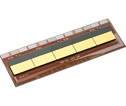
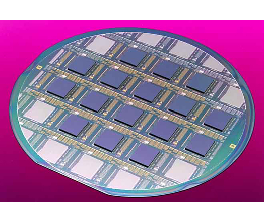
Image sensing applications in several spectrum region as infrared, UV, or X-Rays, comprise one of the fastest growing segments of the semi-conductor industry, largely due to the incredible advances made possible by flip chip technology.
While compression bonding has quickly become the standard technique for IR/FPA applications (successfully achieved on SET bonders), SET is proud to be pioneering the use of advanced reflow techniques that offer many major advantages.
The SET's reflow technique offers carefully controlled thermal cycling and joint shaping capability to reduce stress on the joint and assure reliable connections with a high accuracy rate.
For those who desire high force compression bonding, for example at room temperature, the stable granite base and extreme compression bonding capabilities of SET bonders have no equal in the industry. Meanwhile, SET advances in high-resolution imaging and laser leveling capabilities make high accuracy bonds even more achievable, controlling and guarantying precise parallelism.
Conference proceeding
Process and Equipment Enhancements for C2W bonding in a 3D Integration Scheme
Conference proceeding Download
This paper will review three major areas of process or equipment development surrounding the above problems, namely the issue of throughput enhancement by using a sacrificial adhesive to temporarily tack the dice before collective bonding, the issue of prior or in-situ removal and prevention of surface oxides at the bonding interface, and the issue of local environmental control to reduce particulates and other airborne contaminants. Each of these 3 will be explored with hardware solutions proposed, along with process results on test vehicles or functional devices.
Keith Cooper from SET North America at IWLPC 2011
Chip-to-Wafer Technologies for High Density 3D Integration
Conference proceeding Download
CEA-Leti partnering with SET, STMicroelectronics, ALES and CNRS-CEMES on advanced Chip-to-Wafer technologies for 3D Integration in the frame of the PROCEED project, a 4.2 Million Euros, 24 months project supported by French FIU (Fond Interministeriel Unique). Started in 2009, the goal of the PROCEED project is to demonstrate high alignment accuracy (<1µm) of chip-to-wafer structures made by direct metallic bonding.
Penned by CEA Leti, Minatec campus, CNRS Cemes, ALES, SET, ST Microelectronics and presented at MinaPad 2011
3D-IC Integration using D2C or D2W Alignment Schemes together with Local Oxide Reduction
Conference proceeding Download
3-Dimensional interconnection of high density integrated circuits enables building devices with greater functionality with higher performances in a smaller space. This paper explores the chip-to-chip and chip-to-wafer alignment and the associated bonding techniques such as in-situ reflow or thermocompression with a local oxide reduction which contributes to higher yield together with reduction of the force or temperature requirements.
Gilbert Lecarpentier from SET at Imaps Device Packaging 2011
Flip-chip die bonding: an enabling technology for 3D integration
Conference proceeding
3-Dimensional Integration of Integrated Circuits is a method to build greater functionality into ever-smaller spaces for electronic circuitry, wherein dice of varying sizes, materials, or even application types are electrically and mechanically bonded together.
Keith Cooper from SET North America at IWLPC 2010
Die-to-wafer bonding of thin dies using a 2-step approach: high accuracy placement, then gang bonding
Conference proceeding Download
25 um thick dies, mounted on thick carrier die, were placed on a 300mm landing wafer using the High Accuracy Die Bonder SET-FC300. The bonding process was either Cu/Cu or Cu/Sn with respective pitch of 108 µm and 408 µm...
Gilbert Lecarpentier from SET at Imaps Device Packaging 2010