RF Applications


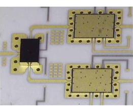
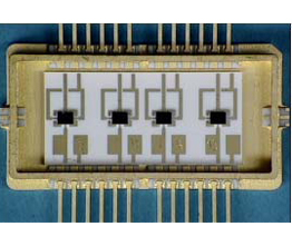
While radio frequency devices have typically not required high accuracy bonding, some recent applications have pointed out the need for finer control of the bonding process.
For certain RF applications such as advanced satellite systems, highly accurate alignment - within 1 µm between chip and substrate - has become desirable. The typical gold-to-gold bonding technique used for RF devices requires inordinately high force at high temperature - a combination that doesn't ordinarily lend itself to high accuracy.
SET Flip Chip Bonders will handle brittle materials safely & easily, even at elevated temperature and high force, while improved control of the force profile throughout the cycle results in better bonding accuracy. Through high performance thermo-compression and leveling capability, SET has made high-end RF connections a reality, with accuracy levels that set a new standard for RF applications.
Conference Proceedings
|
|
|
Process and Equipment Enhancements for C2W bonding in a 3D Integration Scheme |
This paper will review three major areas of process or equipment development surrounding the above problems, namely the issue of throughput enhancement by using a sacrificial adhesive to temporarily tack the dice before collective bonding, the issue of prior or in-situ removal and prevention of surface oxides at the bonding interface, and the issue of local environmental control to reduce particulates and other airborne contaminants. Each of these 3 will be explored with hardware solutions proposed, along with process results on test vehicles or functional devices. |
|
Chip-to-Wafer Technologies for High Density 3D Integration |
CEA-Leti partnering with SET, STMicroelectronics, ALES and CNRS-CEMES on advanced Chip-to-Wafer technologies for 3D Integration in the frame of the PROCEED project, a 4.2 Million Euros, 24 months project supported by French FIU (Fond Interministeriel Unique). Started in 2009, the goal of the PROCEED project is to demonstrate high alignment accuracy (<1µm) of chip-to-wafer structures made by direct metallic bonding. |
|
3D-IC Integration using D2C or D2W Alignment Schemes together with Local Oxide Reduction |
3-Dimensional interconnection of high density integrated circuits enables building devices with greater functionality with higher performances in a smaller space. This paper explores the chip-to-chip and chip-to-wafer alignment and the associated bonding techniques such as in-situ reflow or thermocompression with a local oxide reduction which contributes to higher yield together with reduction of the force or temperature requirements. |
|
Flip-chip die bonding: an enabling technology for 3D integration |
3-Dimensional Integration of Integrated Circuits is a method to build greater functionality into ever-smaller spaces for electronic circuitry, wherein dice of varying sizes, materials, or even application types are electrically and mechanically bonded together. |
|
Die-to-wafer bonding of thin dies using a 2-step approach: high accuracy placement, then gang bonding |
25 um thick dies, mounted on thick carrier die, were placed on a 300mm landing wafer using the High Accuracy Die Bonder SET-FC300. The bonding process was either Cu/Cu or Cu/Sn with respective pitch of 108 µm and 408 µm... |
|
Technical Bulletin
The SET Technical Bulletin N°3, a compilation of technical articles written by some of our customers. Neatly organized and presented, each article provides unique insights into the exciting area of die-to-die and die-to-wafer bonding.
|
|