MCM & LCD


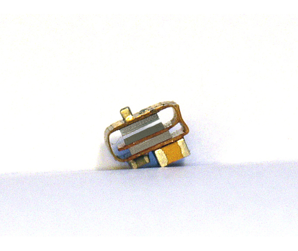
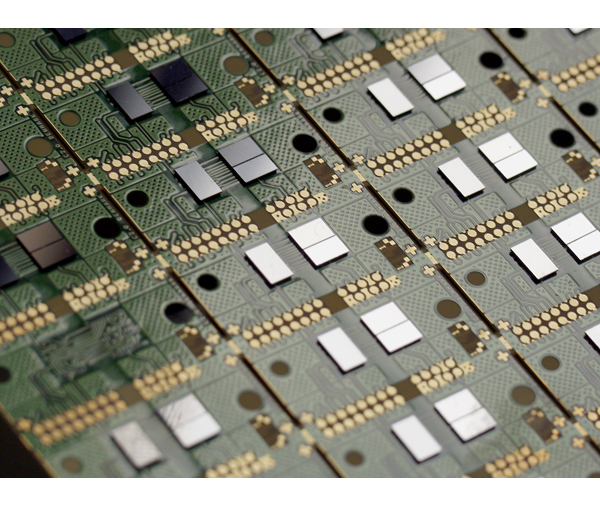
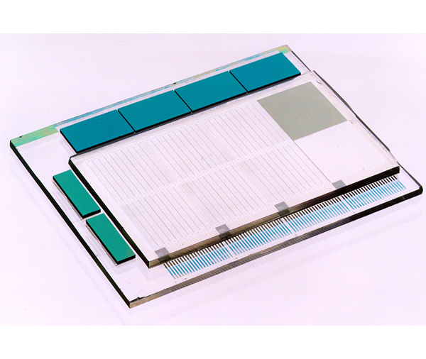
The versatility of SET's Flip-Chip Bonders has proven to be a valuable asset in creating high accuracy alignment levels for multichip modules, compound devices and LCD displays.
Standard MCM applications such as automotive electronics and computers, and LCD/chip-on-glass applications for watches, telephones and other read-out displays have been largely perfected with current flip- chip technology.
Bonding Process
Features such as a flexible user interface, auto alignment capability, and automatic tool exchange enable high-end flip chip bonding applications with maximum ease.
SET's Flip Chip Bonders have process mixing capabilities that allow multiple bonding processes within a single cycle. This provides unsurpassed flip-chip bonding flexibility in a multichip environment with different sized chips in the same cycle.
Conference Proceedings
|
|
|
Process and Equipment Enhancements for C2W bonding in a 3D Integration Scheme |
This paper will review three major areas of process or equipment development surrounding the above problems, namely the issue of throughput enhancement by using a sacrificial adhesive to temporarily tack the dice before collective bonding, the issue of prior or in-situ removal and prevention of surface oxides at the bonding interface, and the issue of local environmental control to reduce particulates and other airborne contaminants. Each of these 3 will be explored with hardware solutions proposed, along with process results on test vehicles or functional devices. |
|
Chip-to-Wafer Technologies for High Density 3D Integration |
CEA-Leti partnering with SET, STMicroelectronics, ALES and CNRS-CEMES on advanced Chip-to-Wafer technologies for 3D Integration in the frame of the PROCEED project, a 4.2 Million Euros, 24 months project supported by French FIU (Fond Interministeriel Unique). Started in 2009, the goal of the PROCEED project is to demonstrate high alignment accuracy (<1µm) of chip-to-wafer structures made by direct metallic bonding. |
|
3D-IC Integration using D2C or D2W Alignment Schemes together with Local Oxide Reduction |
3-Dimensional interconnection of high density integrated circuits enables building devices with greater functionality with higher performances in a smaller space. This paper explores the chip-to-chip and chip-to-wafer alignment and the associated bonding techniques such as in-situ reflow or thermocompression with a local oxide reduction which contributes to higher yield together with reduction of the force or temperature requirements. |
|
Flip-chip die bonding: an enabling technology for 3D integration |
3-Dimensional Integration of Integrated Circuits is a method to build greater functionality into ever-smaller spaces for electronic circuitry, wherein dice of varying sizes, materials, or even application types are electrically and mechanically bonded together. |
|
Die-to-wafer bonding of thin dies using a 2-step approach: high accuracy placement, then gang bonding |
25 um thick dies, mounted on thick carrier die, were placed on a 300mm landing wafer using the High Accuracy Die Bonder SET-FC300. The bonding process was either Cu/Cu or Cu/Sn with respective pitch of 108 µm and 408 µm... |
|
Technical Bulletin
The SET Technical Bulletin N°3, a compilation of technical articles written by some of our customers. Neatly organized and presented, each article provides unique insights into the exciting area of die-to-die and die-to-wafer bonding.
|
|