MEMS Packaging
Nowdays every semiconductor manufacturing technique places restrictions in materials, dimensions, and processing parameters. This places strict design boundaries onto the interdisciplinary nature of MEMS devices.
The ability to integrate mechanical elements with supporting electronics on a micro scale has bolstered micro electromechanical systems (MEMS) as an enabling technology, which has sparked interest in an impressive range of applications. The fabrication of 3-D MEMS devices has certainly benefited from the same equipment and standard processes utilized in the semiconductor industry.
Bonding Process
To get around such limitations, sub-components can be constructed independently by using a combination of traditional processes and novel technologies.
The parts can then be assembled or hybridized to make a more sophisticated device. This scheme, however, presents a number of challenges for handling,maneuvering, aligning and attaching each component.
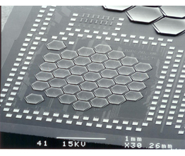
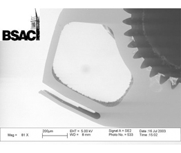
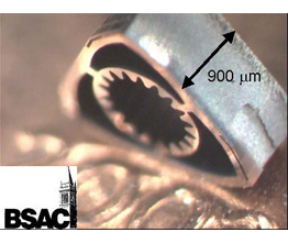
The SET FC150 Automated Device Bonder demonstrated superior ability to handle delicate pieces (down to 200 microns) using vacuum chucks and to align them better than ± 1 µm.
MEMS devices such as adaptive optics system or high end inkjet printer head have been assembled on SET’s Flip-Chip Bonders.