Matrices de plans focaux, capteurs IR, UV et X
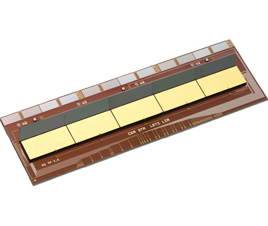
Les applications capteurs d’image dans différentes régions spectrales comme l’infrarouge, l’ultraviolet ou les rayons X, sont un des segments de l’industrie du semi-conducteur de forte croissance, due largement aux énormes avantages de la technologie « flip-chip ».
Alors que l’assemblage par compression devenait la technique standard pour les applications IR/FPA (réalisée avec succès par les Bonders de SET), SET est fière d’être pionnière dans l’utilisation de techniques de refusion, qui présentent de nombreux avantages.
La technique de refusion de SET offre les possibilités de cycles thermiques soigneusement contrôlés et de mise en forme des joints pour réduire les contraintes internes et obtenir des connections fiables avec grande précision.
Pour ceux qui souhaitent des assemblages à hautes forces, par exemple à température ambiante, la base granit rigide et les possibilités de haute compression des Bonders de SET n’ont pas d’équivalent dans l’industrie. En parallèle, les connaissances de SET en imagerie haute résolution et en mesure de parallélisme par laser autorisent les assemblages à haute précision, en contrôlant et garantissant un parallélisme précis.
Publications aux Conférences
Process and Equipment Enhancements for C2W bonding in a 3D Integration Scheme
Publications aux Conférences Télécharger
This paper will review three major areas of process or equipment development surrounding the above problems, namely the issue of throughput enhancement by using a sacrificial adhesive to temporarily tack the dice before collective bonding, the issue of prior or in-situ removal and prevention of surface oxides at the bonding interface, and the issue of local environmental control to reduce particulates and other airborne contaminants. Each of these 3 will be explored with hardware solutions proposed, along with process results on test vehicles or functional devices.
Keith Cooper from SET North America at IWLPC 2011
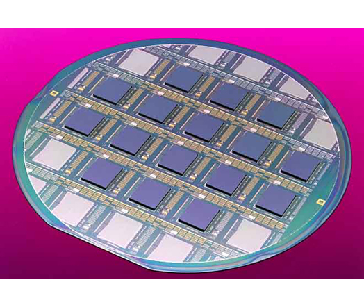
Chip-to-Wafer Technologies for High Density 3D Integration
Publications aux Conférences Télécharger
CEA-Leti partnering with SET, STMicroelectronics, ALES and CNRS-CEMES on advanced Chip-to-Wafer technologies for 3D Integration in the frame of the PROCEED project, a 4.2 Million Euros, 24 months project supported by French FIU (Fond Interministeriel Unique). Started in 2009, the goal of the PROCEED project is to demonstrate high alignment accuracy (<1µm) of chip-to-wafer structures made by direct metallic bonding.
Penned by CEA Leti, Minatec campus, CNRS Cemes, ALES, SET, ST Microelectronics and presented at MinaPad 2011
3D-IC Integration using D2C or D2W Alignment Schemes together with Local Oxide Reduction
Publications aux Conférences Télécharger
3-Dimensional interconnection of high density integrated circuits enables building devices with greater functionality with higher performances in a smaller space. This paper explores the chip-to-chip and chip-to-wafer alignment and the associated bonding techniques such as in-situ reflow or thermocompression with a local oxide reduction which contributes to higher yield together with reduction of the force or temperature requirements.
Gilbert Lecarpentier from SET at Imaps Device Packaging 2011
Flip-chip die bonding: an enabling technology for 3D integration
Publications aux Conférences
3-Dimensional Integration of Integrated Circuits is a method to build greater functionality into ever-smaller spaces for electronic circuitry, wherein dice of varying sizes, materials, or even application types are electrically and mechanically bonded together.
Keith Cooper from SET North America at IWLPC 2010
Die-to-wafer bonding of thin dies using a 2-step approach: high accuracy placement, then gang bonding
Publications aux Conférences Télécharger
25 um thick dies, mounted on thick carrier die, were placed on a 300mm landing wafer using the High Accuracy Die Bonder SET-FC300. The bonding process was either Cu/Cu or Cu/Sn with respective pitch of 108 µm and 408 µm...
Gilbert Lecarpentier from SET at Imaps Device Packaging 2010