焦平面阵列 & 红外、紫外、X光传感器
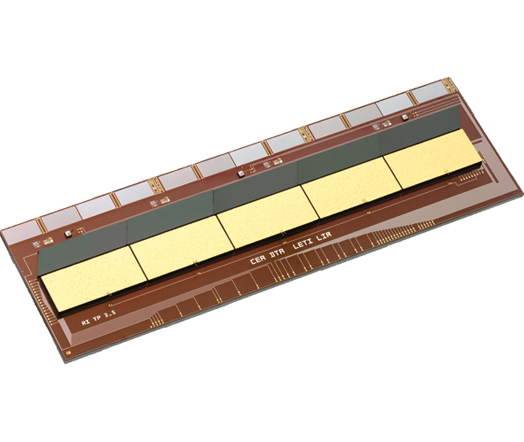
光谱区中的图像感测应用,比如红外、紫外或是X光,是半导体行业中发展最为迅速的市场之一,这主要是由于倒装芯片技术所取得的令人难以置信的进步。
当压力接合已迅速成为红外/焦平面阵列应用(已在SET接合机上成功实现)的标准技术时,SET则光荣地成为了使用具有诸多优点的先进回流焊技术的先行者。
SET的回流焊技术具备精细控制热循环以及焊接凸点成型的能力,从而减少了凸点处的应力,并且确保了在高对准精度下连接的可靠性。
对于那些渴望实现高压接合(比如在室温条件下)的人来说,SET键合机所具有的坚固花岗岩基座以及提供大压力的能力,是行业内的其它产品都无法匹敌的。同时,SET具有领先的高分辨率成像和激光调平能力,这使得高精度接合以及控制和确保精确平行度更易于实现。
会议记录
Process and Equipment Enhancements for C2W bonding in a 3D Integration Scheme
会议记录 下载
This paper will review three major areas of process or equipment development surrounding the above problems, namely the issue of throughput enhancement by using a sacrificial adhesive to temporarily tack the dice before collective bonding, the issue of prior or in-situ removal and prevention of surface oxides at the bonding interface, and the issue of local environmental control to reduce particulates and other airborne contaminants. Each of these 3 will be explored with hardware solutions proposed, along with process results on test vehicles or functional devices.
Keith Cooper from SET North America at IWLPC 2011
Chip-to-Wafer Technologies for High Density 3D Integration
会议记录 下载
CEA-Leti partnering with SET, STMicroelectronics, ALES and CNRS-CEMES on advanced Chip-to-Wafer technologies for 3D Integration in the frame of the PROCEED project, a 4.2 Million Euros, 24 months project supported by French FIU (Fond Interministeriel Unique). Started in 2009, the goal of the PROCEED project is to demonstrate high alignment accuracy (<1µm) of chip-to-wafer structures made by direct metallic bonding.
Penned by CEA Leti, Minatec campus, CNRS Cemes, ALES, SET, ST Microelectronics and presented at MinaPad 2011
3D-IC Integration using D2C or D2W Alignment Schemes together with Local Oxide Reduction
会议记录 下载
3-Dimensional interconnection of high density integrated circuits enables building devices with greater functionality with higher performances in a smaller space. This paper explores the chip-to-chip and chip-to-wafer alignment and the associated bonding techniques such as in-situ reflow or thermocompression with a local oxide reduction which contributes to higher yield together with reduction of the force or temperature requirements.
Gilbert Lecarpentier from SET at Imaps Device Packaging 2011
Flip-chip die bonding: an enabling technology for 3D integration
会议记录
3-Dimensional Integration of Integrated Circuits is a method to build greater functionality into ever-smaller spaces for electronic circuitry, wherein dice of varying sizes, materials, or even application types are electrically and mechanically bonded together.
Keith Cooper from SET North America at IWLPC 2010
Die-to-wafer bonding of thin dies using a 2-step approach: high accuracy placement, then gang bonding
会议记录 下载
25 um thick dies, mounted on thick carrier die, were placed on a 300mm landing wafer using the High Accuracy Die Bonder SET-FC300. The bonding process was either Cu/Cu or Cu/Sn with respective pitch of 108 µm and 408 µm...
Gilbert Lecarpentier from SET at Imaps Device Packaging 2010