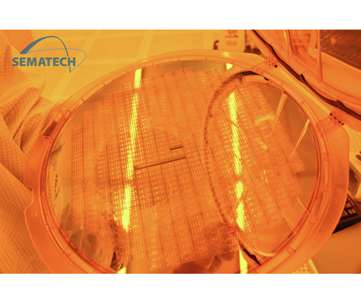
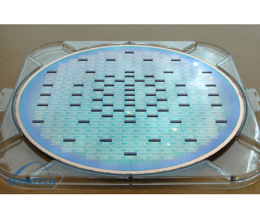
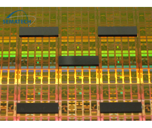
3D Interconnect


Shorten connections lengths to reduce electrical resistance, improve response time as well as reduce power consumption and overall dimensions is one of the main goal to 3D integration.
3D-IC integration enables the high yielding assembly of heterogeneous devices. There are numerous 3D packaging solutions such as:
- interposer,
- direct chip-to-chip bonding or die-to-die bonding,
- chip-to-wafer interconnection.
The placement accuracy requirement varies with the application and the method used to get the signal out of each die. Through-Silicon-Via (TSV) interconnection between chip layers is the focus of the industry today. The optimization of the TSV diameter and pitch is pushing the demands for higher placement accuracy, not only along X and Y axes, but also parallelism between chips.
Bonding Process
High post-bond accuracy and good parallelism between each layer are crucial parameters for 3D stacking. Several bonding processes more dedicated to 3D integration are available on SET’s Flip-Chip Bonders like :
- In-Situ reflow,
- Thermocompression
- Adhesive joining
- Direct metallic bonding
- Etc…
Conference Proceedings
|
|
|
Die-to-Die and Die-to-Wafer Bonding solution for High Density, Fine Pitch Micro-Bumped Die |
Higher density interconnection using 3-Dimensional technology implies a pitch reduction and the use of micro-bumps. The micro-bump size reduction has a direct impact on the placement accuracy needed on the die placement and flip chip bonding equipment. The paper presents a die-to-die and die-to-wafer, high accuracy, die bonding solution illustrated by the flip chip assembly of a large 2x2cm die consisting of 1 million 10µm micro-bumps at 20µm pitch. |
|
Process and Equipment Enhancements for C2W bonding in a 3D Integration Scheme |
This paper will review three major areas of process or equipment development surrounding the above problems, namely the issue of throughput enhancement by using a sacrificial adhesive to temporarily tack the dice before collective bonding, the issue of prior or in-situ removal and prevention of surface oxides at the bonding interface, and the issue of local environmental control to reduce particulates and other airborne contaminants. Each of these 3 will be explored with hardware solutions proposed, along with process results on test vehicles or functional devices. |
|
Chip-to-Wafer Technologies for High Density 3D Integration |
CEA-Leti partnering with SET, STMicroelectronics, ALES and CNRS-CEMES on advanced Chip-to-Wafer technologies for 3D Integration in the frame of the PROCEED project, a 4.2 Million Euros, 24 months project supported by French FIU (Fond Interministeriel Unique). Started in 2009, the goal of the PROCEED project is to demonstrate high alignment accuracy (<1µm) of chip-to-wafer structures made by direct metallic bonding. |
|
3D-IC Integration using D2C or D2W Alignment Schemes together with Local Oxide Reduction |
3-Dimensional interconnection of high density integrated circuits enables building devices with greater functionality with higher performances in a smaller space. This paper explores the chip-to-chip and chip-to-wafer alignment and the associated bonding techniques such as in-situ reflow or thermocompression with a local oxide reduction which contributes to higher yield together with reduction of the force or temperature requirements. |
|
Flip-chip die bonding: an enabling technology for 3D integration |
3-Dimensional Integration of Integrated Circuits is a method to build greater functionality into ever-smaller spaces for electronic circuitry, wherein dice of varying sizes, materials, or even application types are electrically and mechanically bonded together. |
|
Die-to-wafer bonding of thin dies using a 2-step approach: high accuracy placement, then gang bonding |
25 um thick dies, mounted on thick carrier die, were placed on a 300mm landing wafer using the High Accuracy Die Bonder SET-FC300. The bonding process was either Cu/Cu or Cu/Sn with respective pitch of 108 µm and 408 µm... |
|
Technical Bulletin
The SET Technical Bulletin N°3, a compilation of technical articles written by some of our customers. Neatly organized and presented, each article provides unique insights into the exciting area of die-to-die and die-to-wafer bonding.
|
|