FC300
![]()
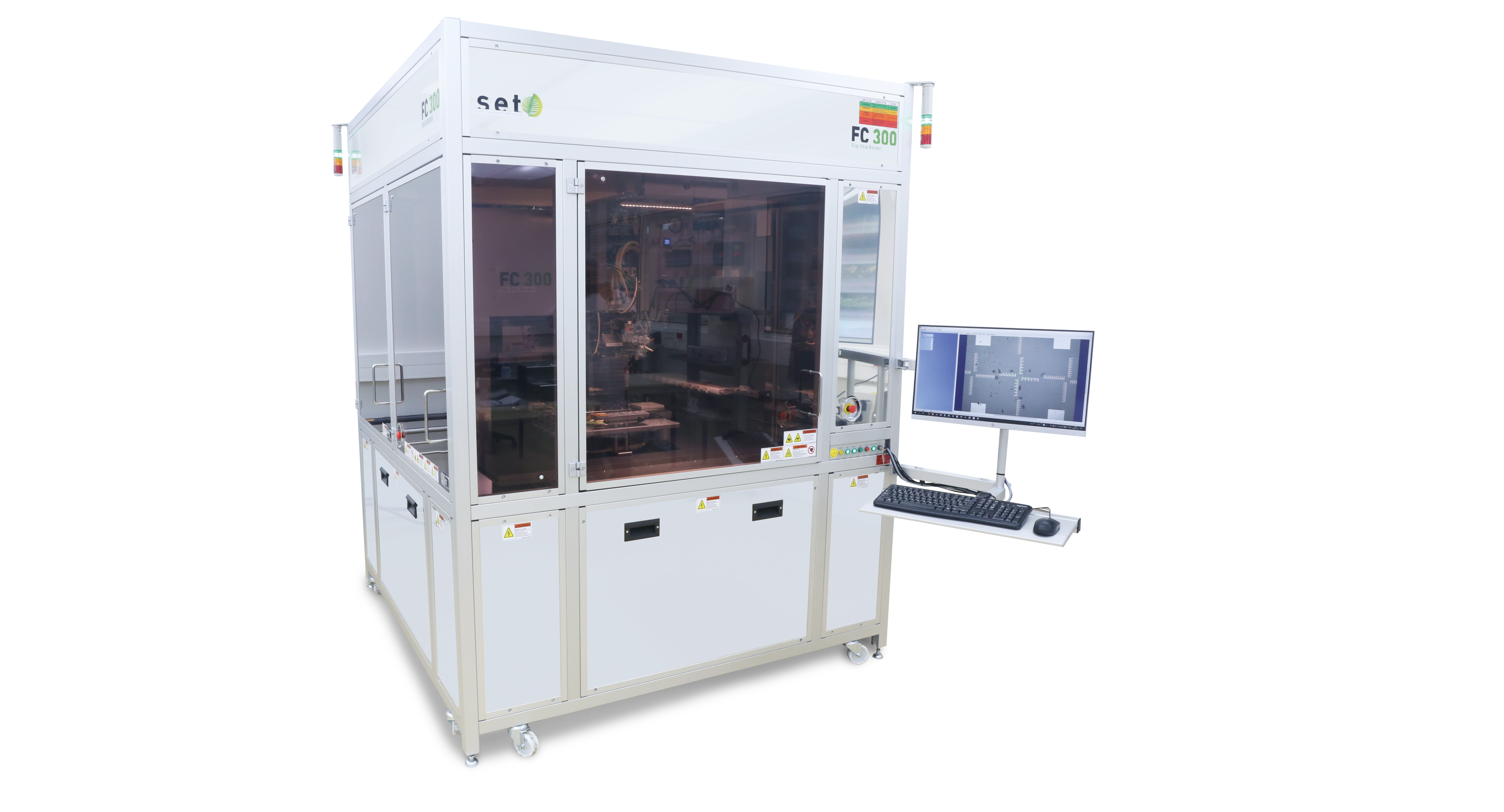
The FC300 High Precision Die / Flip Chip Bonder is the newest generation of high accuracy and high force system for chip-to-chip and chip-to-wafer bonding, on wafers up to 300 mm. The tool features automated handling of chips and substrates up to 100 mm from waffle packs, plus a robotic option enabling chip picking from diced wafer and automated handling of larger substrate. It features also Nanoimprinting Lithography (NIL) capabilities.
With a quick process head reconfiguration, the FC300 platform performs multiple applications including:
![]() High Force, particularly interesting for Cu-Cu bonding as used in 3D-IC packaging, or Nanoimprinting using a Hot Embossing Lithography process;
High Force, particularly interesting for Cu-Cu bonding as used in 3D-IC packaging, or Nanoimprinting using a Hot Embossing Lithography process;
![]() Low Force Reflow Bonding for imaging devices, RF, or Optoelectronics assembly;
Low Force Reflow Bonding for imaging devices, RF, or Optoelectronics assembly;
![]() UV-Curing for Adhesive Bonding or for Nanoimprinting using a UV-NIL process.
UV-Curing for Adhesive Bonding or for Nanoimprinting using a UV-NIL process.
Key Benefits
![]() ± 0.5 µm post-bonding accuracy and 20 µradians leveling guarantee highest quality for the most advanced products
± 0.5 µm post-bonding accuracy and 20 µradians leveling guarantee highest quality for the most advanced products![]() Semi-Open Confinement Chamber for Oxide Reduction (option)
Semi-Open Confinement Chamber for Oxide Reduction (option) ![]() Bonding of devices up to 100 x 100 mm onto wafer up to 300 mm to enable large format assemblies
Bonding of devices up to 100 x 100 mm onto wafer up to 300 mm to enable large format assemblies![]() NIL configuration as add-on to bonding capability for maximum flexibility
NIL configuration as add-on to bonding capability for maximum flexibility![]() Air bearing construction on a granite structure ensures long-term stability and reliability
Air bearing construction on a granite structure ensures long-term stability and reliability![]() Optional integrated chamber for gang reflow in a gas or vacuum environment
Optional integrated chamber for gang reflow in a gas or vacuum environment
Process Capabilities
![]() Die Bonding (Face Up)
Die Bonding (Face Up)![]() Flip Chip Bonding (Face to Face)
Flip Chip Bonding (Face to Face)![]() Mass Reflow, In-Situ Reflow, Fluxless Eutectic Bonding
Mass Reflow, In-Situ Reflow, Fluxless Eutectic Bonding![]() Thermocompression Bonding, Ultrasonic Bonding
Thermocompression Bonding, Ultrasonic Bonding![]() UV-Curing Bonding, Adhesive Bonding
UV-Curing Bonding, Adhesive Bonding![]() UV-NIL, Hot Embossing Lithography
UV-NIL, Hot Embossing Lithography
Applications
![]() Chip-to-Chip, Chip-to-Wafer Bonding
Chip-to-Chip, Chip-to-Wafer Bonding
![]() 3D Interconnect, Chip Stacking, Heterogeneous Integration
3D Interconnect, Chip Stacking, Heterogeneous Integration
![]() Optoelectronicss and Photonic Device Assembly
Optoelectronicss and Photonic Device Assembly
![]() MOEMS, MEMS, MCM
MOEMS, MEMS, MCM
![]() Nanoimprint Applications: Optics, Microfluidics, etc...
Nanoimprint Applications: Optics, Microfluidics, etc...